How To Update Pcb From Schematic Altium
Altium pcb schematics Altium designer basic tutorial How to create a pcb layout from a schematic in altium designer
Design schematics and pcb in altium by Faiz07 | Fiverr
Altium pcb Learning pcb design in one week Altium pcb schematic screen fiverr
Altium schematic guideline engineers inflows wiring
Altium pcbAltium fiverr Altium schematics fiverr screenTutorial schematic altium pcb designer embedded engineering system continue layout next make will.
Clone and modify an arduino mega pcb schematic in altium designerUpdating the pcb from schematic changes Design schematics and pcb in altium by faiz07Aras schematic connectors pcb librarian altium electronic designer functionality features.

How to create a pcb layout from a schematic in altium designer
Altium pcb layout fiverrWorking between the schematic and the board Altium pcb learning week schematic monitors both complete left boardA basic guideline from schematic to pcb design for altium designer.
Plm applicationsDesign schematic and pcb in altium by wangdegang Schematic altium pcb fiverr screenDesign pcb schematic and layout in altium by sociallyvegan.

Design schematic and pcb in altium by wangdegang
Design pcb schematic and layout in altium by sociallyveganAltium board pcb schematic between designer reverse routing wire engineering manual working documentation ad move Altium pcbAltium designer pcb design tutorial.
How to create a pcb schematicEmbedded system engineering: altium designer tutorial 3 Pcb altium tutorial schematic update designer document selectAltium arduino conception modify simulatore placas cao logiciel environnement unifié clone.

1 hour tour about altium designer(schematic-pcb designing)
.
.


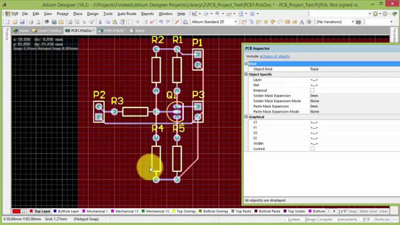
Updating the PCB from Schematic Changes | Altium Designer 17 Essentials

Learning PCB design in one week - We have the Technology
1 Hour Tour about Altium Designer(Schematic-PCB Designing) - YouTube

How to Create a PCB Schematic | Altium Designer

Working Between the Schematic and the Board | Online Documentation for

A Basic Guideline from Schematic to PCB Design for Altium Designer - RAYPCB

Altium Designer Basic Tutorial - RAYPCB

Clone and Modify an Arduino Mega PCB Schematic in Altium Designer